Research
Nanoimprint lithography is an emerging technology for the fabrication of patterns at sub-100 nm resolution. Compared with other lithography tools based on optics, it generates nano-scale patterns with ease at low cost. The equipment itself is much cheaper than EUV, X-ray lithography tools.
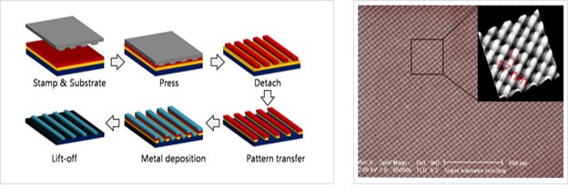
The following schematic diagram shows the procedure how to make metal nanowires by nanoimrpint lithography. It looks simple however; there is a complex of science and engineering inside. With this technique, we fabricated the smallest metal wire array at 17 nm half-pitch
References
"Nanowire circuit fabrication at 17 nm half-pitch by nanoimprint lithography”, G. Y Jung, W. Wu, Z. Yu, S.Y. Wang, Z. Li, R.S. Williams, E. Johnston-Halperin, J.E. Green, B.A. Sheriff, A. Boukai, Y. Bunimovich and J.R. Heath, Nano Letters, 6, 351 (2006) "Fabrication of 34x34 nanoscale crossbar structure by UV-based imprint lithography”, G.Y. Jung, S. Ganapathiappan, D.A.A. Ohlberg, D.L. Olynick, Y. Chen, W.M. Tong, R.S. Williams, Nano letters, 4, 1225 (2004)
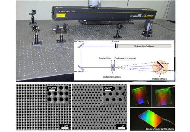
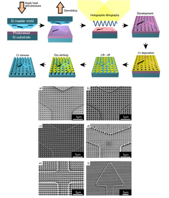
LIL was adopted due to numerous advantages; easy process, short processing time, large area patterning and easy modulation of the density and diameter of periodic hole or pillar patterns. The principle is relatively simple. First, UV laser beam from the He-Cd ion laser goes through the spatial filter consisting of the lens and pinhole, where diffraction limited beam enhancement occurs.
Secondly, the enhanced beam projects an angle bracket, where sample holder and Lloyd mirror are placed perpendicular to each other. On the surface of the sample coated with negative-tone photoresist (PR), one beam from the original UV source and another one reflected from the Lloyd mirror are met and then interference of the two beams occurs. Finally, a 1-dimensional (1D) lined beam having a specific period (pitch) exposes the photoresist.
The pitch size is given by Λ = λUV/2sinθ, where λUV and θ indicate the wavelength of the UV laser (He-Cd laser, 325 nm) and the incident angle, respectively. The periodic formation can also be controlled by irradiating the 1D lined beam with a sample rotated by α; double exposure (α = 0°, 90°) to fabricate a square lattice array, and triple exposure (α = -60°, 0°, 60°) for a hexagonal lattice array. The fabricated PR template can be utilized in various applications including photonic crystal fabrication in light emitting diodes (LEDs) and periodically aligned nanostructure growth.
References
"Simultaneous fabrication of line defects-embedded periodic lattice by topographically assisted holographic lithography" Byung-Yeon Choi, Yusin Pak, Ki Seok Kim, Kwang-Ho Lee, Gun-Young Jung, Nanoscale Res. Lett. 6, 449 (2011)
"Electroluminescence comparison of photonic crystal light-emitting diodes with random and periodic hole structure", Sang-Mook Kim, Ki Seok Kim, Gun Young Jung, Jong Hyeob Baek, Hyun Jeong, Mun Seok Jeong, J. Phys. D: Appl. Phys, 42, 152004 (2009)
he organic electronic devices such as organic light-emitting diode, organic field effect transistor, hybrid solar cell based on polymer film and memories using redox active molecules have drawn attention for their potential applications in the next organic electronics era, due to its availability to the flexible, portable engineering and low cost fabrication. It is important to fabricate metal patterns on the active organic layer without any damage for the reliable device characteristics. However, the conventional photolithography technique involving lift-off process to define top metal patterns is likely to dissolve or degrade the active organic layer by aqueous solutions, resulting in a failure of device fabrication.
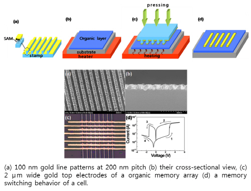
A new non-aqueous direct metal transfer (DMT) technique using a rigid stamp with desirable features is proposed for the metal top contacts on an organic active layer in a single process without destroying the nature of organic active layer. The basic process of DMT is illustrated below. Prior to the DMT process, the stamp surface should be coated with a monolayer of releasing material in vapor phase. A metal layer is deposited on the protruded and recessed areas of the stamp, leaving the stamp sidewalls uncoated. The stamp was then placed onto an organic active film and subjected to a certain pressure and temperature. The metal films deposited on the protruded areas are transported to the organic film surface owing to polymer stickiness during the DMT process, resulting in micron- to nanoscale line patterns. DMT is currently utilized in the field of nonvolatile memory and solar cells in our lab.
References
"Nonaqueous nanoscale metal transfer by controlling the stickness of organic film", Kyeongmi Lee, Seung-Hwan Oh, Nam-Goo Kang, Jae-Suk Lee, Dong-Yu Kim, Heon Lee and Gun Young Jung, Langmuir, 24, 8413 (2008)
Conventional devices using electrons as carriers have approached to their performance limits with scaling down the dimension and/or the continued chip integration; therefore, many scientists believe that light will bring a major breakthrough, being able to travel within a confined dielectric material much faster than the electrons: more information delivery per unit of time. These days, photonic crystal (PhC) structures?with photonic cavities as waveguiding lines or light confinement spots?have been attracting much interest in future photonic devices.
Various techniques have been introduced to fabricate periodic features as well as arbitrary defect lines within them for the light waveguides. However, each technique has drawbacks in addressing several criteria, e.g., large area feasibility, rapid and cost effective process and nanoscale feature generation.We have demonstrated simultaneous fabrication of designed defects within a periodic structure.
For rapid fabrication of periodic structures incorporating nanoscale line-defects at large area, topographically assisted holographic lithography (TAHL) technique, combining the strength of hologram lithography and phase-shift interference, was proposed.Hot-embossing method generated the photoresist patterns with vertical side walls which enabled phase-shift mask effect at the edge of patterns. Embossing temperature and relief height were crucial parameters for the successful TAHL process. Periodic holes with a diameter of 600 nm at a 1 μm-pitch incorporating 250 nm wide line-defects were obtained simultaneously.
References
"Simultaneous fabrication of line defects-embedded periodic lattice by topographically assisted holographic lithography" Byung-Yeon Choi, Yusin Pak, Ki Seok Kim, Kwang-Ho Lee, Gun-Young Jung, Nanoscale Res. Lett. 6, 449 (2011)
As organic electronics era is approaching, there is a need to pattern the functional organic layer. However, the conventional photolithographic technique is not appropriate because the solvents for development and lift-off can attack or dissolve the underlying active organic layer and thus degrade the nature of the organic materials. Therefore, direct solution-processable and printable methods such as micro contact printing (μCP), dewetting, ink-jet printing, screen printing, gravure printing and capillary force lithography (CFL) have been developed for the patterning of organic functional materials. Although each of these non-conventional methods has its own merits, they still require advances in feature size reduction because the solution-processable techniques generally have a difficulty in scaling the pattern size down due to the solution diffusion on a substrate.
We developed new techniques based on surface energy engineering;
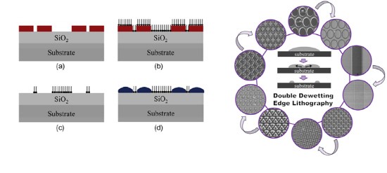
- A substrate with locally varied surface energies, achieved through the novel combination of conventional photolithography and a hydrophobic treatment of the exposed areas. The regions covered by the photoresist remained hydrophilic after the photoresist removal. Thus, an aqueous form of conducting polymer solution spontaneously wet only the defined hydrophilic regions.
- Double-dewetting edge lithography (DDEL). DDEL technique can produce nanoscale polymer patterns by spontaneous double-dewetting phenomena, purely natural process, avoiding any external influences such as pressure and temperature. The DDEL is a simple, cost-effective and easy direct solution patterning method which enables nanoscale polymer edge patterns from various micrometer platforms including lines, angular and irregular shapes.
References
"Solution processable micron- to nanoscale conducting polymer patterning utilizing selective surface energy engineering", Kwang-Ho Lee, Byung-Yeon Choi, Jeong-Woo Park, Seok-Ju Kang, Sang-Mook Kim, Dong-Yu Kim, Gun-Young Jung, Org. Electron, 11, 748-754 (2010)
"Spontaneous nanoscale polymer solution patterning using solvent evaporation driven double-dewetting edge lithography”, Kwang-Ho Lee, Sang-Mook Kim, Huisu Jeong, Gun-Young Jung, Soft Matter, 8, 465-471 (2012)