Research
Graphene is an allotrope of carbon, the structure of which is a two-dimensional (2D) layer with closely packed hexagonal lattices that resemble a honeycomb. Since the first report of discovering exfoliated graphene in 2004, its value to both fundamental physics and electronics has been demonstrated. The most notable of this work resulted in a Nobel Prize in 2010. Because graphene is a zero-bandgap material, it is inherently infeasible as an active material for field-effect transistors. Therefore, most graphene-related research has been focused on the utilization of its high carrier mobility and the transparency of graphene-based electrodes. However, Son et al. theorized that a bandgap opening in graphene could be created by scaling down the width of graphene nanoribbons as narrow as sub-20 nm.
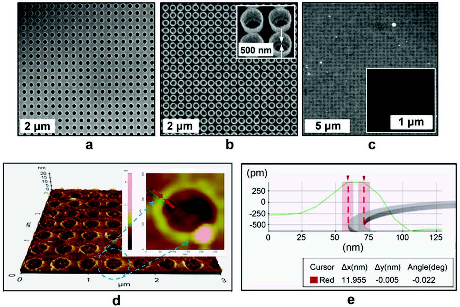
We firstly report the fabrication of large-area, high-density and aligned graphene nanorings (GRNRs) that measure sub-15 nm in width and confirm their successful fabrication and properties by using various measurement tools such as SEM, AFM, TEM and Raman scattering spectroscopy.
References
Large Area Fabrication of Periodic Sub-15 nm Width Single Layer Graphene Nanorings" Yusin Pak, Huisu Jeong, Kwang-Ho Lee, Hui Song, Taehyeon Kwon, Jungsu Park, Woojin Park, Mun-Seok Jeong, Takhee Lee, Sunae Seo, Gun-Young Jung, Adv. Mater., 25, 199-204 (2013)
The ultra-high mobility (theoretically ~200,000 cm2/Vs) and a wide-band photo-detectability (from ultra-violet (UV) to far-IR region) of graphene are very attractive properties for high performance photodetectors. Especially, for the photo-detectability in mid-IR region (λ: 2~10 ㎛), which is highly required in many spectroscopy and sensing applications, graphene is greatly competitive. Compared to the conventional materials such as mercury cadmium telluride (MCT)-based materials or III-V based quantum well infra-red photodetectors (QWIPs), which is used at extremely low temperature (under liquid nitrogen), graphene-devices work at room temperature. On the other hand, a small photo-current generated in a narrow graphene-metal interface is one critical limitation in the realization of the graphene photodetectors.
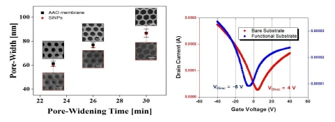
In our group, we developed a novel AAO-based technique for fabricating a tunable sub-100nm nanoporous substrate. This lithography-free technic is utilized to control graphene’s fermi energy, which is finally applied to enhance the responsivity of graphene-photodetectors
References
“A tunable sub-100 nm silicon nanopore array with an AAO membrane mask: reducing unwanted surface etching by introducing a PMMA interlayer”, Namsoo Lim, Yusin Pak, Jin Tae Kim, Youngkyu Hwang, Ryeri Lee, Yogeenth Kumaresan, NoSoung Myoung, Heung Cho Ko, Gun-Young Jung, Nanoscale, 7, 13489-13494 (2015)